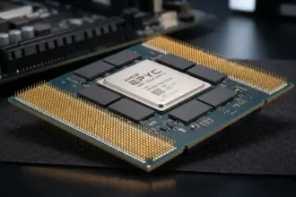


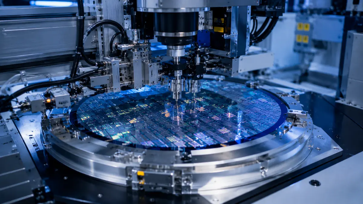
The global artificial intelligence boom has exposed a critical vulnerability in hardware manufacturing that extends far beyond traditional wafer fabrication capacity: advanced semiconductor packaging bottlenecks. As tech giants accelerate the deployment of massive neural network infrastructure, their primary constraint is no longer obtaining raw compute silicon from foundries, but rather securing the specialized back-end assembly required to interconnect high-bandwidth memory with massive tensor processing units.
- The Growing Bottleneck in Advanced Semiconductor Packaging
- Technical Comparison: Intel EMIB vs TSMC CoWoS Architecture
- Yield Rate and Real-World Cost Breakdown: EMIB vs CoWoS
- The Broader Supply Chain Context: HBM and Substrate Shortages
- Supply Chain Diversification: Why Big Tech Needs Intel Foundry
- Can Intel EMIB Fully Solve Google’s CoWoS Shortage?
- Strategic Implications for the Custom Silicon Market
- Future Outlook for Next-Generation Packaging Technologies
- Conclusion
TSMC has long dominated this arena with its proprietary Chip-on-Wafer-on-Substrate technology, creating a single point of failure and severe capacity allocation challenges for hyperscalers. Consequently, major technology companies like Google are forced to evaluate alternative advanced back-end solutions to ensure continuous hardware iteration schedules. Intel Foundry’s proprietary Embedded Multi-Die Interconnect Bridge presents an appealing engineering alternative that could potentially alter the competitive dynamics of modern microchip assembly.
The Growing Bottleneck in Advanced Semiconductor Packaging
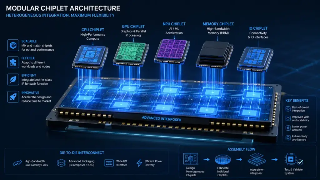
The modern microelectronics landscape has reached a physical threshold where monolithic die scaling yields diminishing returns due to physical wafer layout boundaries and exponential defect costs. To sustain performance gains in high-performance computing, chip architects have systematically shifted away from single massive silicon dies toward modular chiplet architectures. This architectural pivot places semiconductor packaging directly at the center of modern processor design, transforming back-end assembly from a secondary protective housing phase into a primary driver of system compute density and interconnect bandwidth.
The fundamental challenge currently facing artificial intelligence hardware providers centers on back-end capacity allocation rather than front-end EUV lithography throughput. While foundries can print billions of transistors onto silicon wafers with reasonable volume consistency, connecting those logic dies to high-bandwidth memory stacks requires ultra-dense interconnect lines that traditional printed circuit boards simply cannot accommodate. TSMC’s Chip-on-Wafer-on-Substrate has become the industry standard for high-performance AI accelerators, creating an unprecedented concentration of manufacturing reliance in a single geographical region and foundry.
As demand for tensor processing hardware accelerates exponentially, hyperscalers find their deployment schedules constrained by TSMC’s packaging allocation schedules rather than silicon availability. This structural shortage forces cloud infrastructure providers to actively diversify their assembly supply chains, looking closely at competing advanced semiconductor packaging platforms capable of supporting multi-die integration with equivalent signal integrity and thermal performance.
Technical Comparison: Intel EMIB vs TSMC CoWoS Architecture
To evaluate whether alternative manufacturing approaches can alleviate current supply constraints, one must analyze the structural and material differences between competing 2.5D integration platforms. Both solutions aim to solve the identical engineering problem: bridging high-density logic dies to memory stacks with sub-micron line spacing and minimal signal latency.
The TSMC CoWoS Structural Paradigm
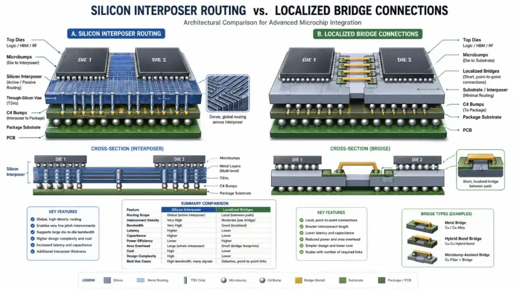
TSMC’s CoWoS technology achieves high interconnect density by utilizing a large, passive silicon interposer layer that sits directly between the underlying package substrate and the active top-level silicon dies. The active logic chip and HBM stacks are mounted onto this shared silicon interposer using microbumps.
- Silicon Interposer Layer: A massive passive silicon slab containing fine-pitch copper interconnects that route signals between adjacent chips.
- Through-Silicon Vias (TSVs): Vertical electrical connections etched through the silicon interposer to carry power and I/O signals down to the organic substrate.
- Substrate Connection: The entire interposer assembly is placed onto a standard package substrate using conventional C4 solder balls.
While this full-interposer methodology provides exceptional interconnect density across large surface areas, it requires significant silicon surface area dedicated solely to passive signal routing. As chiplet dimensions scale upward to accommodate larger compute arrays and additional memory stacks, the required silicon interposer size quickly approaches or exceeds reticle limits, drastically increasing manufacturing complexity and material costs.
The Intel EMIB Engineering Approach
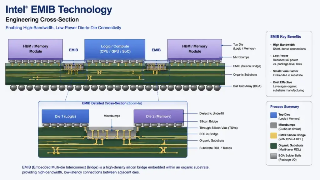
Intel’s Embedded Multi-Die Interconnect Bridge takes a fundamentally different engineering route to achieve ultra-high-density interconnects without relying on a monolithic silicon interposer. Instead of placing all dies on top of a massive passive silicon sheet, EMIB embeds small, ultra-dense silicon bridges directly inside a standard organic package substrate at specific die-edge transition zones.
| Engineering Parameter | TSMC CoWoS-S | Intel EMIB |
| Interconnect Structure | Full-surface passive silicon interposer | Localized silicon bridges embedded in substrate |
| Substrate Type | High-cost full silicon interposer | Standard high-density organic substrate |
| Vertical Connection Method | Through-Silicon Vias (TSVs) through interposer | Direct microbumps to embedded bridge & C4 to substrate |
| Reticle Limit Sensitivity | High (Interposer size constrained by reticle limits) | Low (Bridges are tiny and modular) |
| Material Cost Profile | Higher due to large silicon interposer area | Lower due to localized silicon utilization |
By embedding tiny silicon bridges only where high-density die-to-die or die-to-memory connections are necessary, EMIB drastically reduces the total volume of silicon required for back-end assembly. The surrounding structural substrate remains a conventional, cost-effective organic material, eliminating the need for expensive, large-format silicon interposers and complex Through-Silicon Vias.
Yield Rate and Real-World Cost Breakdown: EMIB vs CoWoS
Evaluating the commercial viability of an alternative packaging platform requires analyzing both yield economics and material cost structures. A solution that appears superior on a theoretical schematic can encounter significant economic friction if production yields lag during high-volume manufacturing runs.
Material Consumption and Substrate Economics
The primary economic advantage of localized bridging lies in structural raw material efficiency. In a full-interposer setup like CoWoS, the cost of the passive silicon interposer scales non-linearly with physical surface area.
- Silicon Surface Utilization: CoWoS uses a passive silicon slab equal to or larger than the combined footprint of all top dies. EMIB uses silicon only along tiny die-to-die border zones.
- Substrate Manufacturing: EMIB allows the use of standard high-density organic substrates, reducing reliance on specialized interposer fabrication lines.
- Thermal Expansion Matching: Eliminating the large silicon interposer simplifies thermal mismatch management between the package and the system board.
“True manufacturing efficiency in 2.5D integration is achieved not by placing more silicon under the entire assembly, but by placing ultra-high-density interconnects precisely where signals cross die boundaries.”
Luna
These material efficiency gains suggest that an optimized semiconductor packaging workflow using localized bridges can offer lower baseline bill-of-materials costs compared to full-interposer methods, provided overall assembly defect rates are strictly controlled.
Analyzing Manufacturing Yield Dynamics
Yield management in multi-die assembly operates under compounded yield curves. When multiple expensive silicon dies are joined onto a single package, a failure in any single component or interconnect link results in scrapping the entire assembled module.
Total Package Yield = (Logic Die Yield) x (Memory Stack Yield) x (Interconnect Assembly Yield)
In a CoWoS process flow, defect density across the large silicon interposer impacts overall yield. If a defect occurs within a TSV or interconnect line on the interposer, all active dies mounted to that interposer are potentially lost.
Conversely, EMIB’s localized bridge approach isolates silicon defect risks to small, low-cost bridge dies. Because these tiny silicon bridges are inherently simple and feature extremely high manufacturing yields prior to substrate insertion, the risk of package failure originating from the interposer material itself is drastically minimized.
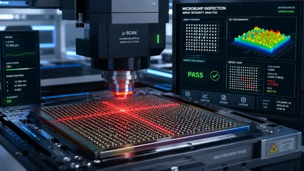
However, embedding tiny silicon bridges into organic substrates with high spatial accuracy introduces its own mechanical challenges. Substrate planarity, microbump placement tolerances, and thermal expansion variance during reflow cycles require extreme precision. Any microscopic shift during the bridge embedding process can result in misaligned microbumps, leading to open circuits or intermittent signal degradation across high-bandwidth memory interfaces.
Read more: Tata Breach and the Secret Development of the iPhone Fold: A Critical Analysis
The Broader Supply Chain Context: HBM and Substrate Shortages
While comparing interposer architectures provides critical engineering insights, packaging capability represents only one layer of a complex, interdependent hardware supply matrix. Transitioning an AI accelerator design from TSMC CoWoS to Intel EMIB does not automatically eliminate all supply chain constraints.
More Read

The High-Bandwidth Memory Bottleneck
Custom tensor processing units rely heavily on High-Bandwidth Memory stacks integrated closely around the central compute dies. HBM manufacturing involves stacking dynamic random-access memory dies vertically using Through-Silicon Vias, followed by rigorous testing and thermal-bond assembly.
- Memory Supplier Concentration: HBM production is heavily concentrated among a small group of memory manufacturers, primarily SK Hynix, Samsung Electronics, and Micron Technology.
- Known Good Die Requirements: Every DRAM layer within an HBM stack must meet strict quality standards to prevent package-level failures after assembly.
- Capacity Pre-Allocation: Global HBM wafer allocation is largely locked into long-term supply contracts months or years in advance.
Even if an alternative foundry offers available capacity within its advanced semiconductor packaging lines, securing sufficient allocations of known-good HBM stacks remains an independent challenge that every hyperscaler must solve separately.
High-Density Ajinomoto Build-Up Film Substrate Limits
Another major constraint affecting high-performance processor manufacturing is the supply of high-density ABF substrates. Both CoWoS and EMIB rely on multi-layer ABF substrates to route power and lower-frequency I/O signals from the chip assembly outward to the motherboard.
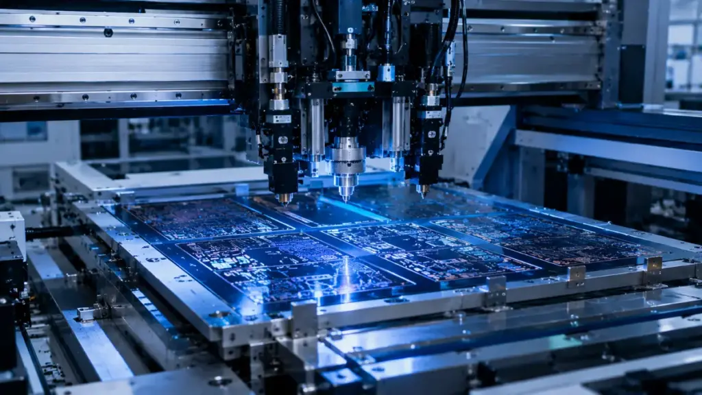
Large-format packages requiring extensive layer counts and tight line-space tolerances place heavy demands on global substrate manufacturing capacity. Consequently, relieving assembly bottlenecks at the interposer stage may simply shift production constraints down to substrate fabrication facilities or memory stacking plants.
Supply Chain Diversification: Why Big Tech Needs Intel Foundry
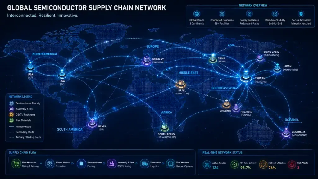
From a corporate risk management perspective, relying exclusively on a single foundry and single geographical region for custom silicon production introduces unacceptable operational vulnerabilities. Tech giants developing in-house silicon are motivated to establish alternative manufacturing pathways for strategic leverage as much as for immediate capacity expansion.
Mitigating Single-Source Risk
The concentration of advanced semiconductor fabrication and back-end packaging within specific regions creates significant exposure to geopolitical tensions, natural disasters, and localized utility disruptions.
“Geographical and operational diversification is no longer a luxury in hardware strategy; it is a fundamental requirement for securing global cloud infrastructure resilience.”
Luna
By qualifying Intel Foundry as a secondary or primary provider for advanced semiconductor packaging, hyperscalers create operational redundancy. This multi-foundry approach ensures that production of vital AI acceleration hardware can continue even if primary manufacturing nodes encounter localized disruptions.
Enhancing Commercial Negotiating Power
Operating within a single-source supplier environment leaves chip designers with limited leverage regarding pricing, allocation priority, and custom architectural modifications.
- Pricing Competition: Introducing a viable competitor to TSMC’s CoWoS framework encourages more competitive packaging service pricing across the industry.
- Allocation Flexibility: Having qualified alternative packaging pipelines allows cloud providers to shift volume production dynamically based on real-time foundry capacity.
- Architectural Co-Development: Working with multiple foundry partners allows chip designers to explore unique structural options tailored to specific custom workloads.
For major infrastructure operators like Google, demonstrating the technical capacity to build high-performance accelerators outside TSMC’s ecosystem provides immense structural leverage during long-term foundry contract negotiations.
Can Intel EMIB Fully Solve Google’s CoWoS Shortage?
Evaluating whether Intel’s EMIB technology can fully alleviate Google’s custom accelerator supply constraints requires a balanced assessment of technical capabilities, manufacturing capacity, and deployment timelines.
Technical Feasibility and Performance Parity
From a pure engineering perspective, EMIB is fully capable of supporting the high-density interconnect requirements of modern tensor processing hardware.
- Interconnect Density: EMIB supports fine microbump pitches capable of delivering massive die-to-die bandwidth density.
- Latency and Power: Short bridge connections maintain low parasitic capacitance, ensuring high signal efficiency and low energy consumption per bit transferred.
- Thermal Management: Eliminating full silicon interposers improves vertical heat dissipation paths, easing overall thermal management design.
These technical characteristics confirm that moving custom AI architectures to an EMIB-based platform does not require sacrificing performance or interconnect efficiency relative to CoWoS.
Realities of High-Volume Production Scaling
However, technical feasibility on test wafers does not automatically translate into instantaneous high-volume supply relief. Transitioning an established chip architecture to a new packaging paradigm requires substantial lead times and process adjustments.
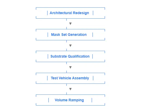
Re-architecting a processor to utilize embedded bridges requires modifying physical floorplans, bump locations, and package substrate design rules. Furthermore, Intel Foundry Services must demonstrate sustained high-volume manufacturing stability and yield consistency across extended production runs to match the decades of operational maturity built into TSMC’s packaging lines.
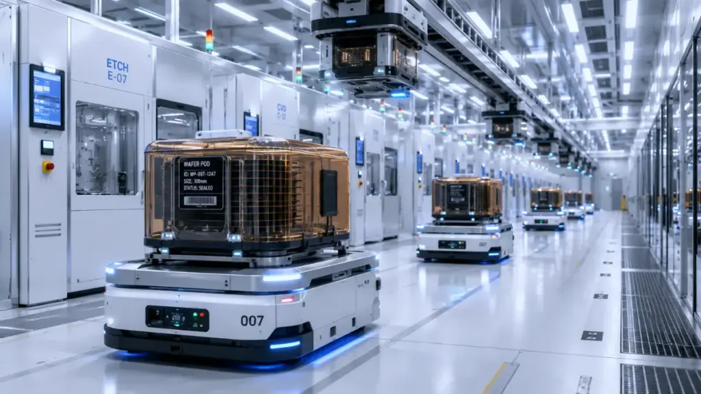
Therefore, while EMIB provides a technically viable and strategically essential relief valve for hyperscaler supply constraints, it represents a mid-to-long-term structural solution rather than an overnight quick fix for immediate hardware shortages.
Strategic Implications for the Custom Silicon Market
The emergence of competitive alternatives in back-end assembly signals a broader transformation within the global semiconductor industry. Packaging has officially evolved from a standardized commodity service into a primary battleground for foundry differentiation and architectural innovation.
The Shift Toward Open Foundry Ecosystems
As multi-die chiplet designs become universal, foundries are forced to adopt more flexible assembly business models.
- Mix-and-Match Chiplets: Future hardware platforms may feature logic dies printed at one foundry integrated alongside memory stacks and peripheral chiplets packaged by another provider.
- Standardized Die Interfaces: Industry initiatives around open die-to-die interconnect standards are reducing software and physical barriers to cross-foundry packaging integration.
- Decoupled Packaging Services: Foundries are increasingly offering stand-alone advanced packaging services for customer dies printed on external foundry wafers.
This modular evolution allows hardware developers like Google to optimize their manufacturing strategies by selecting the most cost-effective and available provider for each individual layer of their hardware stack.
Future Outlook for Next-Generation Packaging Technologies
Looking beyond current 2.5D integration platforms, the semiconductor industry is already pioneering next-generation packaging frameworks designed to support the exponentially growing compute requirements of future artificial intelligence models.
Transitioning to True 3D Stacking Architectures
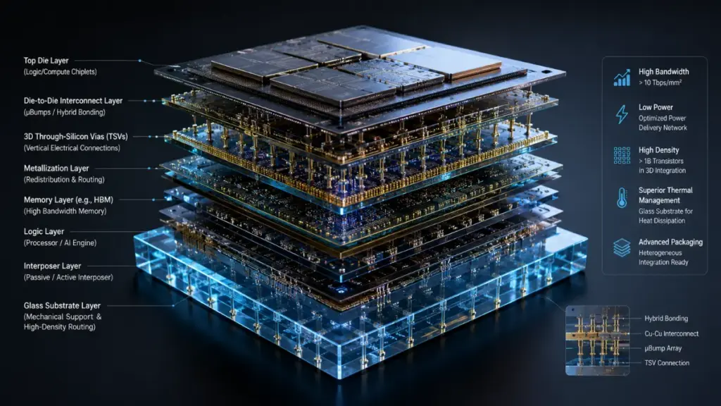
While 2.5D methods like EMIB and CoWoS place dies side-by-side on a shared substrate or interposer, 3D vertical stacking technologies mount logic directly on top of logic or memory.
- Intel Foveros: Utilizes direct vertical face-to-face die bonding to minimize interconnect distance and latency to absolute physical limits.
- TSMC SoIC: Enables ultra-fine pitch direct copper-to-copper hybrid bonding without intermediate microbumps.
- Glass Substrates: Foundries are actively developing glass package substrates to replace organic materials, offering superior mechanical stability, thermal endurance, and feature density.
The Long-Term Competitive Landscape
The competition between major foundries to master advanced semiconductor packaging will ultimately benefit hyperscalers and custom chip designers. As Intel, TSMC, and Samsung heavily invest in expanded packaging capacity and architectural research, hardware developers will gain unprecedented operational flexibility, lower structural production risks, and accelerated hardware deployment cadences.
Conclusion
Intel’s EMIB offers a powerful, engineering-sound alternative to TSMC’s heavily constrained CoWoS platform. By utilizing localized embedded silicon bridges within cost-effective organic substrates, EMIB delivers high interconnect bandwidth and low latency while optimizing material efficiency and component defect risks. While adopting a new packaging pipeline requires significant redesign lead times, qualification testing, and parallel supply chain adjustments for HBM and substrate allocations, Google’s strategic engagement with Intel Foundry represents a crucial step toward diversifying global AI hardware production. Advanced semiconductor packaging is no longer merely an assembly step—it is the strategic cornerstone of modern cloud compute infrastructure independence.
LEAVE A COMMENT BELOW TO GET FREE EXPERT CONSULTATION OR FOLLOW OUR WEBSITE THE COUCH INSIDER TO UPDATE THE LATEST KNOWLEDGE.